Meshy AI 3D Data Side Business: Complete Guide to Pricing, Marketplaces, Copyright, and Post-Processing (2026 Edition)
swiftwand swiftwand.ai
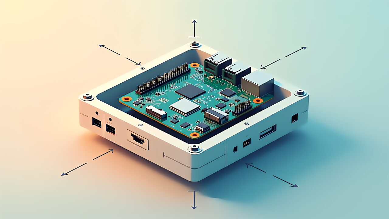
The soldering is done. The board works on your desk. And then it sits there — a bare PCB with wires sprouting in every direction, waiting for the box that never gets designed. Enclosure design is the step nobody teaches: schematics class covers how to read a circuit, but not how far apart the mounting holes on a Raspberry Pi 5 actually are. This article breaks the journey from bare board to closed box into seven steps, with the specific numbers you need at each one and the reasoning behind them.
3D printing gives us one huge advantage over injection molding here. In the world of machined tooling, a design mistake costs weeks and thousands of dollars to fix. In ours, it costs a few cents of filament and a few hours of reprinting. That freedom is exactly why a structured process matters — without one, you spend that freedom reprinting the same box five times.
| Step | What you decide | Output |
|---|---|---|
| 1. Measure | Real dimensions of board and parts, connector positions and heights | A dimension memo |
| 2. Internal layout | Board orientation, part clearances, cable routing | Minimum internal size |
| 3. Shell and walls | Internal size + clearance + wall thickness, corner radii | Outer dimensions |
| 4. Openings | Connector holes, switch holes, vent positions | Face cutouts |
| 5. Mounting | How the board is held: bosses, inserts, standoffs | Internal features |
| 6. Lid | Split line, mating faces, fasteners | A two-part (or more) design |
| 7. Verify | Gauge prints, interference checks, trial assembly | A fix list |
The order matters: each step’s output feeds the next, so decisions stop colliding. One refinement worth adopting immediately — although verification is listed last, insert a small gauge print right after step 3. Printing one business-card-sized test plate before committing to the full enclosure eliminates most of the late-stage rework. More on that below.
Everything starts with measurement, and the best source is the official mechanical drawing. For the Raspberry Pi 5, the official drawing (RP-008347-DS-1) specifies a board of 85 × 56 mm, mounting holes on a 58 × 49 mm pitch, hole diameter 2.7 mm, offset 3.5 mm from the board edge. If your board has published mechanicals, use them; if not, measure the functional dimensions only — outline, hole positions, connector centerlines, and the tallest component. Don’t forget board thickness: a typical FR-4 board is around 1.6 mm, and omitting it shifts every opening by 1–2 mm.
Internal layout is a set of trade-offs: putting all connectors on one face simplifies the cutouts but complicates cable routing; stacking two boards saves footprint but hurts height and cooling. A single hand-drawn cross-section on paper at this stage pays for itself many times over.
The outer shell comes down to three numbers. First, wall thickness: the manufacturing service Protolabs Network (formerly Hubs) recommends a minimum wall of 2 mm for enclosures. Printers can produce walls down to 0.8 mm, but that is a “printable” limit, not a “survives being used as a box” limit. A 2 mm wall also happens to suit a 0.4 mm nozzle nicely — two perimeters plus infill fill it cleanly.
Second, clearance: the same design guide recommends 0.5 mm of clearance around all internal components. This is not a vague margin — it comes from error budgets. Desktop FDM dimensional accuracy is commonly quoted at ±0.5% with a floor of ±0.5 mm, so a 100 mm box routinely lands half a millimeter off per side.
Third, corners: run a 2–3 mm fillet on outside corners and a small radius on inside corners. Both warping and cracking drop noticeably, because sharp inside corners are textbook stress concentrators. With these three numbers fixed, the outer size is arithmetic: internal size = parts + 0.5 mm clearance; external size = internal + 2 mm wall × 2.
Openings and mounting features generate most of the late rework. For ports and plugs, Protolabs Network recommends 2 mm of clearance — 1 mm per side — around the actual cable or connector body, not the receptacle spec. For screws, the guide’s numbers are simple: add 0.25 mm to the screw diameter for clearance holes, subtract 0.25 mm for self-tapping holes, and keep at least one hole-diameter of plastic around every screw hole. Bosses need a flat seat and a fillet at the root; the height should clear whatever protrudes from the underside of the PCB — solder joints and clipped pin-header legs routinely stick out 3 mm, so measure them and add 1 mm.
Before committing to a five-hour enclosure print, spend thirty minutes on a gauge: a small plate carrying your actual cutouts and hole sizes stepped in 0.1 mm increments. Fit the real cables and screws, note which sizes work, and transfer the winners into the model. Printing the full box three times versus printing a 30-minute gauge twice and the box once — the arithmetic speaks for itself. Keep the results in a notes file; after a few projects you won’t need the gauge at all, because you’ll have your own calibration data for your printer and filament.
PLA prints beautifully, but check the thermal numbers before defaulting to it. Polymaker’s technical data sheet for PolyLite PLA lists a glass transition temperature of 61°C (DSC, 10°C/min), a Vicat softening temperature of 63°C (ISO 306), and heat deflection temperatures of 60°C at 0.45 MPa and 58°C at 1.8 MPa. The melting point is 150°C, but that is not the number that matters: around 60°C the material starts to soften and will deform under load. A sunny windowsill, a closed car, or a warm power supply can all reach that range. Answer three questions at the planning stage — indoors or out? direct sun? internal heat source? — and the PLA-versus-PETG-or-better decision makes itself.
Of the seven steps, the part AI genuinely accelerates is describing the shape. Give an LLM your measured dimensions and ask for parametric OpenSCAD — mounting-hole pitch as variables, bosses placed in a loop — and it will produce reusable code in minutes. What AI cannot do is guarantee the dimensions: it has never held your board, and it will happily generate geometry that collides with reality. The division of labor is clear: AI writes the form, the human owns the measurements and the verification.
A few classics worth pre-empting. Underside protrusions: solder points and pin-header legs stick out about 3 mm, so boss height should be measured protrusion plus 1 mm. Tight insertion at openings: a 0.5 mm chamfer on the rim solves most of it. Mismatched holes between base and lid: define every coordinate as a variable in one place and reference it from both parts — the moment you type the same number twice, it will eventually diverge. And if your board runs hot, think about airflow from the start rather than drilling vents into a finished print.
Enclosure design is seven steps: measure, lay out, shell, openings, mounting, lid, verify. The core numbers: 2 mm minimum walls, 0.5 mm clearance around components, 1 mm per side around ports, screw clearance holes at diameter +0.25 mm, self-tapping holes at −0.25 mm, one hole-diameter of material around every screw hole, and a gauge print before the real one. Measure the actual board, keep every dimension in one variable, and the box will close on the first try far more often than not.